Applications
- Radar Systems (antenna azimuth)
- Navigation Systems (gyrocompass, speedlog, course, pitch, and roll)
- Industrial Processes (position, velocity)
- Meteorology Instruments (wind speed and direction)
- Many Others
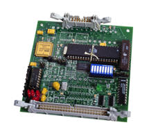
Card Layout:
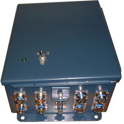
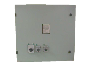
The Data Acquisition System (DAS) is a stand alone system which interfaces to several types of analog and digital inputs and outputs (I/O). An onboard microcontroller controls the processing of these signals to provide conversion to user requested outputs. An optional LCD display enables display of raw or converted data. The DAS is capable of interfacing to two synchro/resolver, two serial, sixteen digital and two analog interfaces and is factory configurable to customer requirements for easy field installation. DAS is also available in rugged EMI/EMC enclosures.
Features:
- NEMA-0183 Compatible
- Optional LCD Display
- 90V, 11.8V Synchro, 6.8V Resolver
- RS-232, RS-422, RS-423, RS-485, MIL-STD-188C Protocols
- Custom Serial Data Formats and Frequencies are available upon request
| Technical Specification | ||
| Parameter | Value | Units |
| Power Input | 115/230 | Volts AC |
| 20/10 | Milliamps | |
| Temperature Range | ||
| Operating Temperature | 0 to +50 | °C |
| Storage Temperature | -65 to +150 | °C |
| Inputs/Outputs | ||
| Synchro | 90 and 11.8 | Volts |
| 0-2000 | Hertz | |
| Resolver | 6.8 | Volts |
| 0-2000 | Herts | |
| Serial Message | NMEA-0183 | |
| Serial Protocol | RS-232/422/423/485 or MIL-STD-188C | |
| Digital | 16 bit | TTL |
| 5 | Volts DC | |
| Analog | +/- 10 | Volts |
| Accuracy | +/- 4 | Arc Minutes |
| Physical Characteristics | ||
| 8.0 x 10.0 x 4.0 | Inches | |
| 20.3 x 25.4 x 10.2 | Centimeters | |
Inputs/Outputs
Inputs and outputs are available on circular connectors provided with the DAS. Inputs and outputs are listed below:
Serial Interfaces
Serial data interfaces use the standard National Marine Electronics Association(NMEA) message formats NMEA-0183 as shown below. This I/O is available in RS-232, RS-422, RS-423, RS-485, or MIL-STD-188C protocols. Standard output update rate is once per second. Custom serial data formats and frequencies are available upon request.
Serial baud rate selection and checksum checking is determined from the configuration switches at power up or reset. Selectable baud rates include: 2400, 4800, 9600, 19,200 and 38,400 bits per second. Default data output is 9600, 8 bits, no parity, and one stop bit (9600, 8, N, 1). Table 3 defines the switch position for the available baud rates.
| DAS BAUD RATE SELECTION AND CHECKSUM VALIDATION | ||||||||
| BAUD RATE (bits per sec) | Configuration Switch S1 | |||||||
| 1 | 2 | 3 | 4 | 5 | 6 | 7 | 8 | |
| 2400 | 1 | 1 | 0 | X | X | X | X | X |
| 4800 | 0 | 0 | 1 | X | X | X | X | X |
| 9600 | 1 | 0 | 1 | X | X | X | X | X |
| 19200 | 0 | 1 | 1 | X | X | X | X | X |
| 38400 | 1 | 1 | 1 | X | X | X | X | X |
| 1 = off, 0 = on, X = Don’t Care | ||||||||
NMEA-0183 Format
The DAS can be factory programmed for any NMEA-0183 data format. Default data format is as follows:
$PTBBG,AAA.AA,BB.B,C,D,EEE.E,FF.F,G,HA*CSCRLF
$ – start of message ascii character 24 Hex
PT – Proprietary message
BBG – BBG Incorporated
AAA.AA – channel 1 angular information (ex: 045.01)
BB.B – channel 1 analog information (ex: 08.4)
C – channel 0-3 hexidecimal digital information (ex: 7) Note: 7 = 0111
D – channel 4-7 hexidecimal digital information (ex: E) Note: E = 1110
BBG – BBG Incorporated
EEE.EE – channel 2 angular information (ex: 270.24)
FF.F – channel 2 analog information (ex: 10.0)
G – channel 8-11 hexidecimal digital information (ex: 5) Note: 5 = 0101
H – channel 12-15 hexidecimal digital information (ex: E) Note: A = 1010
A – validity (A = valid, V = Invalid)
* – ascii character 2A Hex
CS – checksum (8 bit XOR of characters between $ and *
CR – carriage return
LF – Line feed
Synchro/Resolver Interfaces
Synchro/Resolver Inputs:
Inputs are jumper selectable for synchro or resolver signals and can be configured for any desired voltage by a simple chip/resistor replacement. Synchro or resolver inputs are fused and transient protected. Standard voltages include 90Vrms, 26 Vrms, and 11.8Vrms synchro inputs and 6.8 Vrms resolver inputs over the frequency range of DC to 40kHz. Custom voltages are available upon request. Please specify desired voltage when ordering DAS.
Synchro/Resolver Outputs:
Outputs are factory configurable for synchro or resolver signals at any required voltage and frequency. Please specify desired voltage and frequency when ordering card. Synchro/resolver outputs are reference powered.
Analog Interfaces
Analog Inputs:
Inputs are factory configurable for full scale ranges of -10V to +10V. Custom ranges are available upon request. Please specify desired voltage range when ordering UCE.
Connector List
J1 SERIAL
I/O CONNECTOR TYPE: MS3470L10-6S
| PIN NO | SIGNAL | PIN NO | SIGNAL |
| A | TXD422+ (OUTPUT) | D | RXD422- |
| B | TXD422+ (OUTPUT) | E | GND |
| C | RXD422- (INPUT) | F | SPARE |
J2 SYNCHRO
I/O CONNECTOR TYPE: MS3470L10-6P
| PIN NO | SIGNAL | PIN NO | SIGNAL |
| A | CHAN 1 R1 (INPUT) | D | CHAN 1 S2 (OUTPUT) |
| B | CHAN 1 R2 (INPUT) | E | CHAN 1 S3 (OUTPUT) |
| C | CHAN 1 S1 (OUTPUT) | F | SPARE |
J3 ANALOG
I/O CONNECTOR TYPE: MS3470L8-33S
| PIN NO | SIGNAL | PIN NO | SIGNAL |
| A | CHAN 1 SIGNAL (INPUT) | C | SPARE |
| B | CHAN 1 RETURN (INPUT) |
J4 DIGITAL
I/O CONNECTOR TYPE: MS3470L12-8S
| PIN NO | SIGNAL | PIN NO | SIGNAL |
| A | CHAN 0 (INPUT) | E | GND |
| B | CHAN 1 (INPUT) | F | SPARE |
| C | CHAN 2 (INPUT) | G | SPARE |
| D | CHAN 3 (INPUT) | H | SPARE |
J5 DIGITAL
I/O CONNECTOR TYPE: MS3470L12-8S
| PIN NO | SIGNAL | PIN NO | SIGNAL |
| A | CHAN 4 (INPUT) | E | GND |
| B | CHAN 5 (INPUT) | F | SPARE |
| C | CHAN 6 (INPUT) | G | SPARE |
| D | CHAN 7 (INPUT) | H | SPARE |
J6 AC POWER
I/O CONNECTOR TYPE: MS3470L8-98P
| PIN NO | SIGNAL | PIN NO | SIGNAL |
| A | 115/230VAC LINE (INPUT) | C | CHASSIS GND |
| B | 115/230VAC LINE RETURN (INPUT) |
J7 SYNCHRO
I/O CONNECTOR TYPE: MS3470L10-6PW
| PIN NO | SIGNAL | PIN NO | SIGNAL |
| A | CHAN 2 R1 (INPUT) | D | CHAN 2 S2 (OUTPUT) |
| B | CHAN 2 R2 (INPUT) | E | CHAN 2 S3 (OUTPUT) |
| C | CHAN 2 S1 (OUTPUT) | F | SPARE |
J8 ANALOG
I/O CONNECTOR TYPE: MS3470L8-33SW
| PIN NO | SIGNAL | PIN NO | SIGNAL |
| A | CHAN 2 SIGNAL (INPUT) | C | SPARE |
| B | CHAN 2 RETURN (INPUT) |
J9 DIGITAL
I/O CONNECTOR TYPE: MS3470L12-8SX
| PIN NO | SIGNAL | PIN NO | SIGNAL |
| A | CHAN 8 + (INPUT) | E | CHAN 10 + (INPUT) |
| B | CHAN 8 – (INPUT) | F | CHAN 10 – (INPUT) |
| C | CHAN 9 + (INPUT) | G | CHAN 11 + (INPUT) |
| D | CHAN 9 – (INPUT) | H | CHAN 11 – (INPUT) |
J10 DIGITAL
I/O CONNECTOR TYPE: MS3470L12-8SY
| PIN NO | SIGNAL | PIN NO | SIGNAL |
| A | CHAN 12 + (INPUT) | E | CHAN 14 + (INPUT) |
| B | CHAN 12 – (INPUT) | F | CHAN 14 – (INPUT) |
| C | CHAN 13 + (INPUT) | G | CHAN 15 + (INPUT) |
| D | CHAN 13 – (INPUT) | H | CHAN 15 – (INPUT) |


